| Oct 06, 2023 |
|
(Nanowerk Information) Perovskite-based photo voltaic cells are seen as potential successors to the prevalent silicon cells due to their cost-effectiveness and excellent efficiency. Latest analysis has showcased perovskite photovoltaic cells with enhanced optoelectronic properties. One of many predominant obstacles to their wider adoption is decreasing optical losses in these next-generation cells.
|
Key Takeaways
|
|
Photovoltaics have seen a 1000-fold improve in put in capability over the previous 20 years, with silicon-based cells nearing their effectivity limits.
Perovskite-based cells provide over 26% effectivity and an economical manufacturing course of.
Scientists launched a nanoimprinting methodology to create environment friendly anti-reflective constructions on perovskite cells, enhancing scalability and efficiency.
This new strategy preserves the perovskite’s integrity and helps adaptable cell architectures.
The tactic is conducive to tandem configurations of silicon and perovskite, signaling future improvements in photovoltaic effectivity.
|
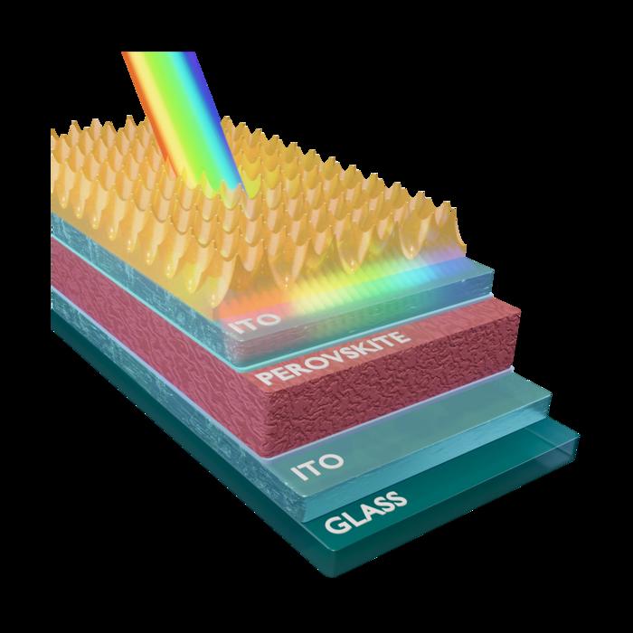 |
| The visualization of the manufactured honeycomb texture for the perovskite photo voltaic cell (Picture: Maciej Krajewski, College of Physics on the College of Warsaw)
|
The Analysis
|
|
Photovoltaics has skilled a major growth over the previous 20 years, contemplating each panel effectivity and the put in capability, which has elevated worldwide by a staggering 1000 instances since 12 months 2000. Silicon has been probably the most generally used materials for producing photovoltaic panels, but presently cells primarily based on this ingredient are approaching their bodily effectivity limits. Subsequently, scientists are actively exploring progressive options focused at enhancing cell effectivity and concurrently enabling cheaper and extra environmentally pleasant manufacturing.
|
|
Perovskite-based cells meet each of those standards, providing effectivity above 26%, ease and cost-effectiveness in manufacturing utilizing well-established chemical strategies. At present, quite a few analysis institutes worldwide are engaged on enhancing their effectivity and resistance to atmospheric circumstances. One of many challenges they’re going through is the mixing of perovskite cells with silicon cells whereas concurrently decreasing losses from reflection and parasitic absorption.
|
|
To attenuate these losses, silicon cells are sometimes etched with extremely corrosive chemical brokers, a course of that creates microscopic pyramid sample on the floor, successfully decreasing the reflection of your entire machine, thereby growing the present generated by the machine. Sadly, perovskites are delicate to many chemical substances, which is why much less efficient planar anti-reflective coatings utilized by much less invasive sputtering have been employed to this point.
|
|
In analysis revealed in Superior Supplies and Interfaces (“Curler Nanoimprinted Honeycomb Texture as an Environment friendly Antireflective Coating for Perovskite Photo voltaic Cells”), scientists used the nanoimprinting methodology to create an environment friendly anti-reflective construction with honeycomb-like symmetry atop the perovskite photo voltaic cell. This method permits the manufacturing of nanometer-scale constructions on very massive surfaces, exceeding 100 cm2.
|
|
“This strategy ensures scalability within the manufacturing strategy of large-surface gadgets, which is essential within the context of the pressing want for power transformation towards renewable power sources,” says Msc Maciej Krajewski, a researcher from the College of Physics on the College of Warsaw. Such modified samples show increased effectivity in comparison with cells utilizing beforehand employed planar anti-reflective layers.
|
|
Along with enhancing effectivity, one other vital discovering from the revealed work is that the appliance process for this layer doesn’t injury the perovskite, opening the opportunity of utilizing different constructions tailor-made to the particular cell architectures.
|
|
Till now, scientists utilized related anti-reflective constructions as individually ready layers, which have been transferred in one other technological course of that was inevitably small-scale and prone to damaging the energetic layer. By using the direct nanoimprinting methodology, it turns into potential to fabricate your entire machine on a big scale and in a single technological course of, which is essential for decreasing the general machine prices.
|
|
Moreover, the utilized methodology is appropriate with a tandem configuration, i.e., combining silicon and perovskite cells, opening up a wholly new prospects for its software. Consequently, there’s the potential for straight transferring the process to rising photovoltaic architectures, which might result in additional enhancements in effectivity. The revealed outcomes pave the best way for brand spanking new photovoltaic gadgets with excellent optoelectronic properties, using nanoimprinting methods of their manufacturing.
|

