| Oct 18, 2023 |
|
(Nanowerk Information) Particle accelerators are essential instruments in all kinds of areas in business, analysis and the medical sector. The area these machines require ranges from a couple of sq. meters to massive analysis facilities. Utilizing lasers to speed up electrons inside a photonic nanostructure constitutes a microscopic different with the potential of producing considerably decrease prices and making gadgets significantly much less cumbersome.
|
|
Till now, no substantial vitality good points had been demonstrated. In different phrases, it has not been proven that electrons actually have elevated in pace considerably. A workforce of laser physicists at Friedrich-Alexander-Universit�t Erlangen-N�rnberg (FAU) has now succeeded in demonstrating the primary nanophotonic electron accelerator � similtaneously colleagues from Stanford College.
|
Key Takeaways
|
|
Researchers have efficiently developed a nanophotonic electron accelerator, basically a “particle accelerator on a chip.”
The know-how makes use of lasers to speed up electrons inside a photonic nanostructure, providing a extra compact and doubtlessly cheaper different to traditional particle accelerators.
The workforce used the alternating section focusing (APF) methodology to information electrons and achieved a 43% acquire in vitality over half a millimeter.
This improvement might pave the way in which for extremely moveable accelerators, with purposes in medical imaging and radiotherapy.
To make the know-how sensible for medical use, the vitality acquire have to be elevated by roughly 100 occasions, based on the researchers.
|
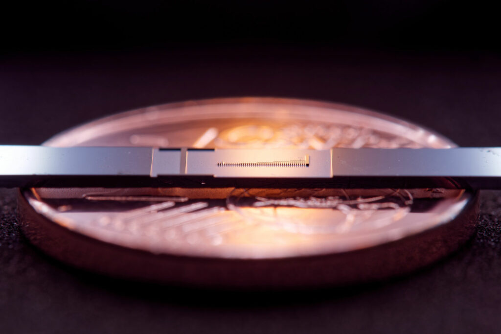 |
| For the primary time, FAU researchers have succeeded in measurably accelerating electrons in constructions which are only some nanometers in dimension. Within the image you may see the microchip with the constructions and, as compared, a 1 cent coin. (Picture: FAU, Julian Litzel)
|
The Analysis
The researchers from FAU have now printed their findings within the journal Nature (“Coherent nanophotonic electron accelerator”).
|
|
When individuals hear �particle accelerator�, most will most likely consider the Giant Hadron Collider in Geneva, the roughly 27 kilometer lengthy ring-shaped tunnel which researchers from across the globe used to conduct analysis into unknown elementary particles. Such enormous particle accelerators are the exception, nonetheless. We usually tend to encounter them somewhere else in our daily lives, for instance in medical imaging procedures or throughout radiation to deal with tumors. Even then, nonetheless, the gadgets are a number of meters in dimension and nonetheless somewhat cumbersome, with room for enchancment by way of efficiency.
|
|
In a bid to enhance and reduce the dimensions of present gadgets, physicists across the globe are engaged on dielectric laser acceleration, also called nanophotonic accelerators. The constructions they use are merely 0.5 millimeters in size, and the channel the electrons are accelerated by is just roughly 225 nanometers in width, making these accelerators as small as a pc chip.
|
|
Particles are accelerated by ultrashort laser pulses illuminating the nano-structures.
|
|
�The dream software could be to put a particle accelerator on an endoscope so as to have the ability to administer radiotherapy straight on the affected space throughout the physique,� explains Dr. Tom� Chlouba, one of many 4 lead authors of the just lately printed paper.
|
|
This dream should be far past the grasp of the FAU workforce from the Chair of Laser Physics led by Prof. Dr. Peter Hommelhoff and consisting of Dr. Tom� Chlouba, Dr. Roy Shiloh, Stefanie Kraus, Leon Br�ckner and Julian Litzel, however they’ve now succeeded in taking a decisive step in the correct course by demonstrating the nanophotonic electron accelerator.
|
|
�For the primary time, we actually can discuss a particle accelerator on a chip,� enthuses Dr. Roy Shiloh.
|
Guiding electrons + acceleration = particle accelerator
|
|
Simply over two years in the past the workforce made their first main breakthrough: they succeeded in utilizing the alternating section focusing (APF) methodology from the early days of acceleration concept to manage the move of electrons in a vacuum channel over lengthy distances (“Physicists management the move of electron pulses by a nanostructure channel”). This was the primary main step on the way in which in direction of constructing a particle accelerator. Now, all that was wanted to achieve main quantities of vitality was acceleration.
|
|
�Utilizing this method, we’ve got now succeeded not solely in guiding electrons but in addition in accelerating them in these nano-fabricated constructions over a size of half a millimeter,� explains Stefanie Kraus.
|
|
While this may not sound like a lot of an achievement to many, it’s a enormous success for the sphere of accelerator physics. �We gained vitality of 12 kiloelectron volts. That could be a 43 p.c acquire in vitality,� explains Leon Br�ckner.
|
|
With a purpose to speed up the particles over such massive distances (when seen from the nano scale), the FAU physicists mixed the APF methodology with specifically developed pillar-shaped geometrical constructions.
|
|
This demonstration is just the start, nonetheless. Now the goal is to extend the acquire in vitality and electron present to such an extent that the particle accelerator on a chip is enough for purposes in medication. For this to be the case, the acquire in vitality must be elevated by an element of roughly 100.
|
|
�With a purpose to obtain increased electron currents at increased energies on the output of the construction, we must develop the constructions or place a number of channels subsequent to one another,� Tom� Chlouba explains the subsequent steps of the FAU laser physicists.
|
